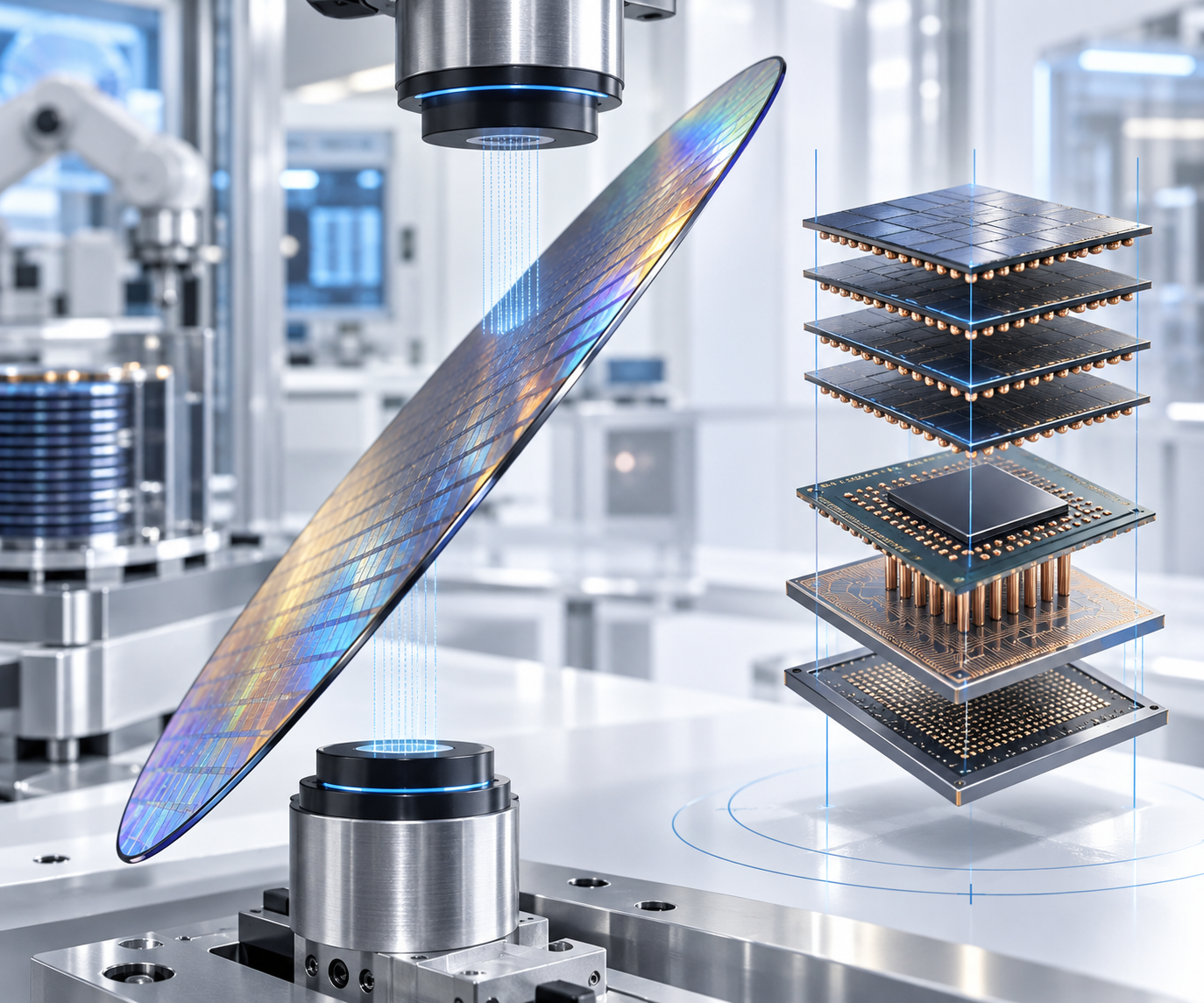
MTI Instruments Proforma systems help semiconductor manufacturers monitor backside processing for HBM, chiplets and next-generation computing devices
LOCKPORT, IL, UNITED STATES, September 22, 2026 /EINPresswire.com/ — Vitrek is highlighting the growing importance of precision wafer-thickness measurement as semiconductor manufacturers expand production of GPU/AI Engines, High-bandwidth Memory, Traditional CPUs, Programmable Logic and Power Semiconductors.
Advanced packaging technologies combine logic, memory, interposers and specialized dies within tightly controlled structures. To meet package-height and integration requirements, wafers often undergo backside grinding, polishing and other thinning operations.
As wafers become thinner, they are increasingly susceptible to breakage, warpage and uneven material removal. These conditions can affect handling, bonding, stacking and assembly—after considerable value has already been added to the wafer.
“Advanced packaging has made wafer thickness and geometry critical process variables,” said Todd Stukenberg, Vitrek President, “Manufacturers need reliable data between process steps so they can detect variation before wafers reach costly packaging operations.”
The MTI Instruments Proforma 300i and Proforma 300iSA use proprietary capacitance-based technology to provide non-contact wafer measurements. The manual Proforma 300i supports point-based thickness and total-thickness-variation measurements. The semi-automated Proforma 300iSA provides programmable scanning and mapping for thickness, total thickness variation, bow, warp and flatness.
Published specifications include thickness accuracy of ±0.25 µm and resolution of 0.05 µm. The Proforma 300iSA can collect as many as 1,000 measurement points per minute, depending on its configuration and measurement routine.
By inspecting wafers between grinding and polishing stages, manufacturers can identify non-uniform material removal, monitor changes in wafer geometry and correct process drift before bonding or package assembly.
As AI and HPC applications drive wider adoption of HBM, 2.5D and 3D integration, reliable thickness data can help manufacturers improve process control, reduce scrap risk and protect downstream manufacturing value.
For more information about MTI Instruments semiconductor-metrology systems, visit Vitrek.com or stop by booth # 5245 at Semicon West, October 13-15 in San Francisco, CA.
Suzy Abbott
Vitrek
+1 815-838-0005
email us here
Visit us on social media:
LinkedIn
Facebook
YouTube
Legal Disclaimer:
EIN Presswire provides this news content “as is” without warranty of any kind. We do not accept any responsibility or liability
for the accuracy, content, images, videos, licenses, completeness, legality, or reliability of the information contained in this
article. If you have any complaints or copyright issues related to this article, kindly contact the author above.

Media gallery